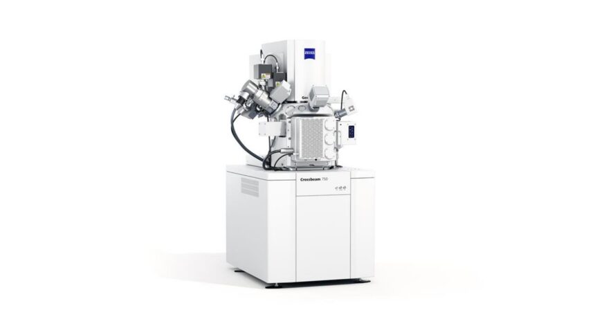
Zeiss has unveiled the new Zeiss Crossbeam 750 focused ion beam-scanning electron microscope (FIB-SEM), optimised for demanding sample preparation. It can provide a live, high-resolution “see while you mill” view, under any imaging and milling conditions, enabling immediate feedback and eliminating milling interruptions to produce uniform first-pass transmission electron microscopy (TEM) lamellae and precise FIB cross sections.
For advanced semiconductor and materials workflows, Zeiss Crossbeam 750 FIB-SEM, with Gemini 4 electron optics, can provide background-free, real-time endpointing and sub-nanometer precision for TEM lamellae and high-fidelity 3D analysis. It is suitable for analysing leading-node logic, memory devices, nanofabrication, and 3D volume imaging. For materials research and life sciences, Zeiss Crossbeam 750 speeds up 3D tomography acquisition times by providing a larger field of view with reduced distortion.
Dr Thomas Rodgers, senior director of market strategy, head of business sector electronics, Zeiss Microscopy, said, “Zeiss Crossbeam 750 was designed around one core principle: Our customers should not have to stop milling to see where in their sample they are working. Our new high-dynamic-range (HDR) Mill + SEM capability maintains a clear, high-resolution SEM view at any FIB condition, from rapid milling with high FIB currents down to fine polishing at 0.5 kV. This real-time clarity, paired with Gemini 4 electron optics, allows customers to fine-tune processes as they work, reducing rework, improving yield and delivering highly uniform lamellae on the first pass.”
“See while you mill”
As semiconductor device architectures shrink and complexity increases, from fin field-effect transistor (finFET) to gate-all-around (GAA), complementary field-effect transistor (CFET), and emerging 2D materials, precise, real-time control during FIB processing has become essential. Zeiss Crossbeam 750 addresses this need by maintaining a high-resolution SEM view during milling, even at low landing energies and at tilt.
The system allows users to observe FIB-sample interactions in real time, fine-tune thinning and polishing steps as they occur, and hit nanometer-scale endpoints on the first attempt, enabling consistent lamella quality for leading-node logic, memory device, and backside power delivery network workflows.
Driving scientific discovery
The Zeiss Crossbeam 750 FIB-SEM is critical to materials science workflows, including uniform TEM lamella preparation, atom probe tomography (APT) sample preparation, nanofabrication, and high-fidelity 3D volume imaging. For life sciences and materials research, the undistorted large field-of-view of the Zeiss Crossbeam 750 and its stable low-kV performance enhance signal-to-noise and reduce acquisition time.